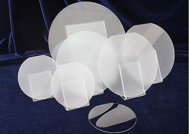
The GaN substrate market is anticipated to be valued at USD 5,420.5 million in 2023. Additionally, it is expected to experience a steady growth rate of 9.7% over the next ten years, ultimately reaching a significant value of USD 13,721.9 million by 2033. This growth can be attributed to the persistent focus on environmentally friendly transportation initiatives, particularly the promotion of green vehicles.
Gallium Nitride (GaN) substrate is a semiconductor material with distinct advantages when compared to conventional semiconductor materials like Silicon, Silicon Carbide, Aluminum, Sapphire, and others.
GaN is typically grown as a thin film on substrates such as Sapphire, Silicon, and Silicon Carbide. Currently, GaN on sapphire dominates the market share, but it’s anticipated that GaN on Silicon Carbide (SiC) will experience the most rapid growth in applications like LEDs and power electronics.
Reach Out to Our Sales Team Now and Discover the Insights You Need to Succeed!
Owing to a lot of advantages over all the other traditional substrates, GaN Substrate is one of the most emerging substrates in the industry and holds a high growth potential. High electron mobility, low switching losses, and fewer lattice mismatches are some of the key advantages of the GaN Substrate, which are leading to the worldwide adoption of GaN Substrate, mainly in the industries such as optoelectronics and power electronics.
Currently, the GaN Substrate holds authority in LEDs possessing a share of nearly 70% of market revenue, while power electronics products are in an evolving stage. Other applications of GaN Substrate also involve inverters (& converters), RF devices, power supply modules and motor drives which are expected to evolve rapidly in the market.
GaN Substrate is a semiconductor material, whose advantages are evident in comparison to the other conventional semiconductor materials such as Silicon, Silicon Carbide, Aluminium, Sapphire, and others. The GaN material is a thin film which is grown on other materials like Sapphire, Silicon, and Silicon Carbide.
Out of which, the GaN on sapphire currently holds for most of the share, but SiC is expected to evolve at the fastest rate among others, in the LEDs and Power electronics segment.
Global Market of GaN Substrate: Drivers and Restraint
Wider band gap, high break-down voltage, larger critical electric field, and higher thermal conductivity are some of the key factors leading to a rapid shift of industry manufacturers from silicon technology to GaN substrate.
These properties let the GaN Substrate material operate at much higher voltages, work at high switching frequencies, and increase its ability to handle higher power density, thereby offering enhanced power efficiency, which are the key requirements of power amplifiers and applications pertaining to optoelectronics, they are the captivating interest in the R&D fields of these industries.
GaN Substrate also exceeds the limit of their counterpart Si devices in applications like Schottky diodes, FETs, HEMTs, and other advanced transistors and lets them operate efficiently at much higher voltage levels. These are the key factors that result in gaining attraction for GaN Substrate in the market, with the LED applications being the key drivers holding a share of nearly 70% of revenue in the market for the bulk gallium nitride (GaN) market.
As these devices help reduce conduction and switching losses and offer higher efficiency in electronic systems, gradually they are entering a new segment of applications, namely power amplifiers. These applications of GaN Substrate are in an evolving stage but are anticipated to show substantial growth in the upcoming years.
Key Market Players:
- Cree Inc.
- Kyocera Corp.
- MonoCrystal
- Sumco Corp.
- Sumitomo Electric Industries
- 10+
- Saint Gobain Ltd.
- Mitsubishi Chemical Corporation
- Texas Instruments Incorporated
- GaN Systems Inc.
- MTI Corporation
A Full Report on the Market:
https://www.futuremarketinsights.com/reports/gan-substrate-market
GaN Substrate Market Segmentation:
By Size:
- 2-inch
- 4-inch
- 6-inch
- Higher than 6 Inches
By Type:
- Sapphire
- Si
- SiC
- GaN
By Substrate Production Process Type:
- Hydride Vapor Phase Epitaxy-based (HVPE)
- Ammonothermal Growth-based
- Metal-Organic Chemical Vapor Deposition (MOCVD)
By End User:
- Healthcare
- Automotive
- Military and Communication
- General Lighting
- Consumer Electronics
- Power Generation
- Telecom
By Region:
- North America
- Latin America
- Europe
- Asia Pacific
- Middle East & Africa
About Future Market Insights (FMI)
Future Market Insights, Inc. (ESOMAR certified, recipient of the Stevie Award, and a member of the Greater New York Chamber of Commerce) offers profound insights into the driving factors that are boosting demand in the market. FMI stands as the leading global provider of market intelligence, advisory services, consulting, and events for the Packaging, Food and Beverage, Consumer Technology, Healthcare, Industrial, and Chemicals markets. With a vast team of over 400 analysts worldwide, FMI provides global, regional, and local expertise on diverse domains and industry trends across more than 110 countries.
Contact Us:
Future Market Insights Inc.
Christiana Corporate, 200 Continental Drive,
Suite 401, Newark, Delaware – 19713, USA
T: +1-845-579-5705
For Sales Enquiries: sales@futuremarketinsights.com
Website: https://www.futuremarketinsights.com
LinkedIn| Twitter| Blogs | YouTube

